A buffer is a simple logic gate that may not immediately seem useful. That is because when the input is off the output is off. When the input is on the output is on. The difference is that when the output is on the signal strength and quality will be improved. How the buffer changes the input signals varies depending on the type of buffer and buffer design.
Emitter Follower Buffer
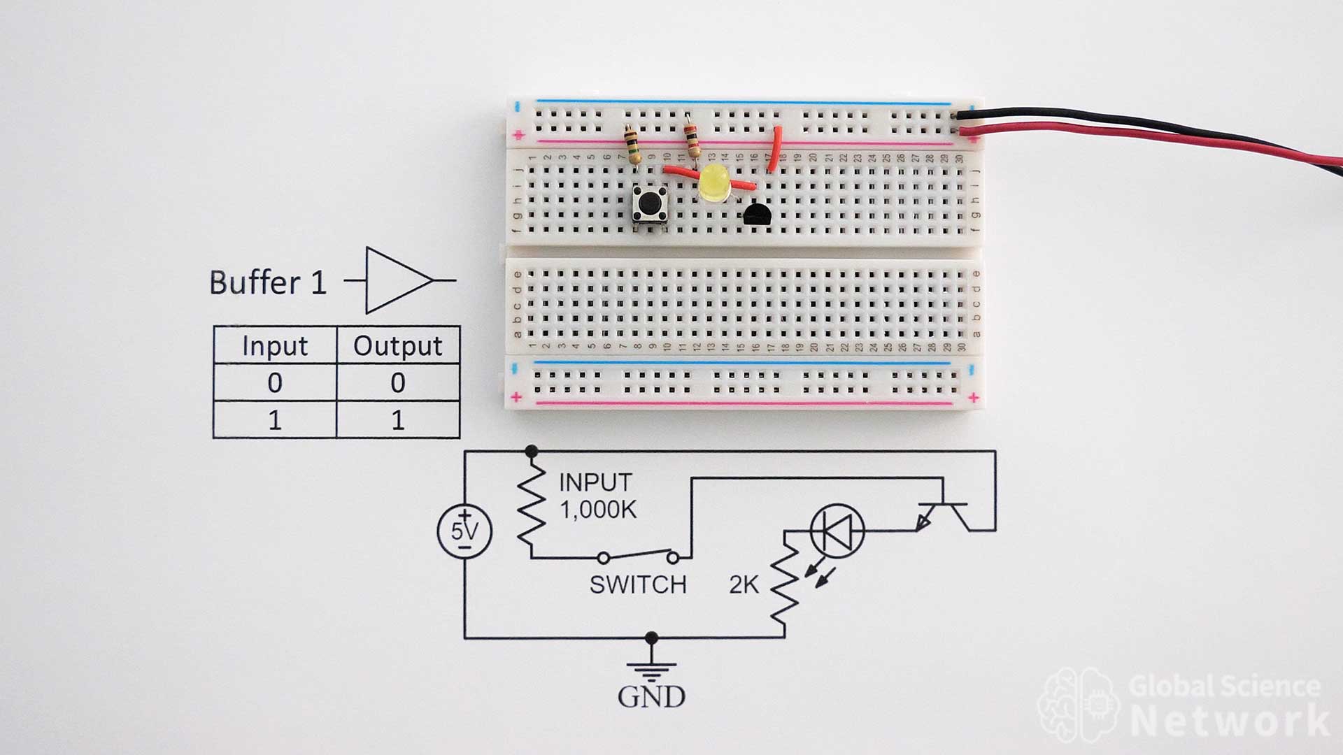
The first buffer is set up with the output on the emitter side of the transistor. This is similar to an emitter-follower buffer. However, a true emitter follower is made to condition an AC signal and includes a voltage divider for the base input and two capacitors to filter the signal.
This circuit works by feeding a low-current signal into the base of the transistor. In the example, the 1,000K resistor makes the current value .005 mA. The transistor amplifies the current by allowing up to 100 times more current to flow from the collector to the base than is flowing from the base to the collector. This allows enough current to light the LED. Before the input signal was only .005 mA which is not enough to provide light.
If the buffer is not sending an output the LED could be on the collector side of the transistor. In this case, the red wire going to positive voltage would be switched with the 2K resistor, and the 2K resistor going to the ground would be switched with a black wire.
This video shows how to build all types of logic gates. At 11:13 the digital buffers and amplifier buffers are discussed in detail.
Buffer 1 Truth Table
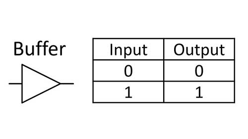
A buffer symbol is a triangle with an input and output line. The truth table for a buffer is simple. When the input is 0 the output is 0 and when the input is 1 the output is 1. A buffer is useful because it can take a high-impedance signal with a low current and turn it into an output with low impedance and high current. This allows the circuits to be isolated but correlated and acts in a similar way to a relay or optocoupler.
Buffer 1 Circuit Diagram
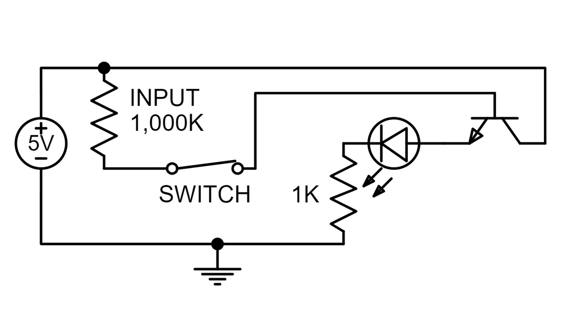
The circuit diagram above shows the component level drawing of buffer 1. When the switch is closed the low current flows from the 1,000K resistor and into the base of the transistor. The collector is connected directly to the 5-volt power supply. A 330 ohm to 2K resistor is added on the path to the ground to ensure the current is limited. With such a low current going into the base this is not actually required but it is good practice to always have a current-limiting resistor added when using an LED.
Buffer 2
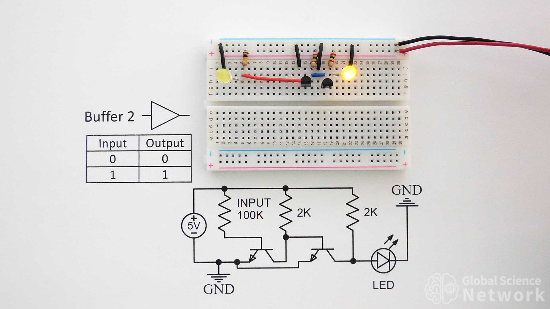
Buffer 2 is another configuration and its design makes it easy to send the output signal to other circuits. The circuit design is basically two inverters. Buffer 1 does work at lower current values than buffer 2. However, buffer 2 is set up more like all the other types of digital logic gates with the output being sent from the collector side of the transistors.
Buffer 2 Circuit Diagram
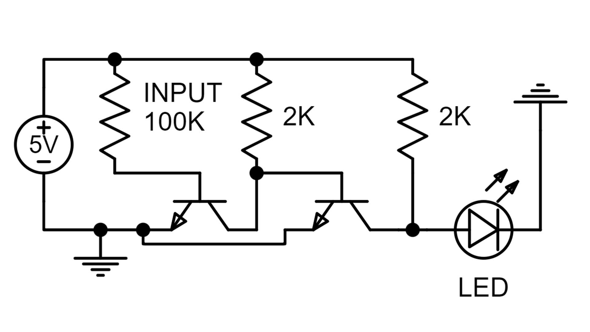
The component level circuit diagram for buffer 2 is shown above. This circuit will work with an input resistor value of 100K. If a 100k resistor value is used the buffer does not work properly. This is because the voltage drop across the middle 2K resistor is 4.28 volts allowing .72 volts to go into the base of the second transistor. The second transistor will turn on if the voltage is above .6 volts causing the LED to turn OFF. So this buffer does work in many cases but like all buffers is limited to how low of a signal it can work with.
Tri-State Buffer
A tri-state buffer has a data input, a enable input, and an output. The control input allows the buffer to enter a high-impedance output state. This is often used when data is being sent over a bus. The high impedance state allows the output to not be high or low and act like it is disconnected from the circuit. A tri-state buffer enable input is also called a control input and can set the output to high impedance during the high or low signal. These buffers are called the active high tri-state buffer or the active low tri-state buffer.
Active High Tri-State Buffer Truth Table
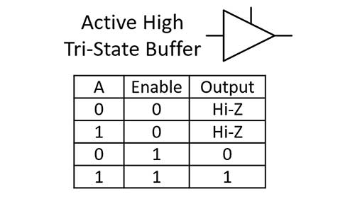
For the active high case, the signal will actually be on or off when the enable input is on. When the enable input is off the output will be in high impedance mode.
Active Low Tri-State Buffer Truth Table
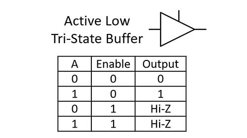
For the active low case, the signal will actually be on or off when the enable input is off. When the enable input is on the output will be in high impedance mode.

Cody started the Global Science Network with the idea people should be focusing more time, energy, and resources on useful projects. He has a bachelor’s degree in aerospace engineering and a master’s degree in mechanical engineering. Cody has worked for the US federal government, a university, a large corporation, small businesses, and for himself. He has done human brain computer interface research and is currently working towards creating non-biological human consciousness.